 Mini Review
Studies on Thickness Uniformity, Stress Modulation, as well as Transport Behavior in Sputtered thin Films of TiN
WANG Junbao1, XIAO Weiwei2, WANG Lu1, LIANG Lanju1 and GAO Ju1*
1College of Optoelectronic Engineering Zaozhuang University, Shandong province Zaozhuang, China
2College of Media Zaozhuang University, Shandong province Zaozhuang, China
GAO Ju, College of Optoelectronic Engineering Zaozhuang University, Shandong province Zaozhuang, 277160, China.
Received Date:April 21, 2023; Published Date:May 11, 2023
Abstract
The applications of microelectronic devices based on TiN compound require superior quality of film growth. In this work the thickness uniformity, stress modulation, as well as transport behavior of TiN thin films have been studied systemically. The films were grown on monocrystalline silicon by magnetron sputtering. The effects of sputter power, argon/nitrogen ratio and sputter pressure on the formation of thin films were investigated by using X-ray fluorescence spectrometer, X-ray diffractometer, stress measuring instrument, and four probe technique. The results showed that the sputter power may play an important role on the crystal orientation of the film. The argon/nitrogen ratio and sputter pressure could also affect the properties of grown TiN films. By optimizing the preparation parameters, uniform TiN films with high compressive stress and high resistivity were obtained, which is promising for wide applications in microelectronic devices and sensors.
Keywords:Magnetron sputtering; TiN film; Thickness uniformity; Stress; Resistivity
Introduction
Titanium nitride (TiN), a member of the group IV transition metal nitrides, possess a NaCl face-centered cubic crystal structure. In the TiN structure, the orbital energy level of N is lower than Fermi level. It makes the movement of free electrons being similar to that of electrons in metal orbitals. TiN is formed by the combination of covalent and metallic bonds. Thus, it may show the characteristics of both covalent and metallic crystals, like high hardness, high melting point, excellent thermal and electrical conductivity, high temperature chemical stability, biological compatibility, corrosion resistance, etc. TiN coatings have been widely used in high temperature ceramics, bearing gears, optical components, capacitors, integrated circuits, aerospace and other fields [1-3]. In practical industrial applications, TiN thin films are often prepared by physical vapor deposition (PVD) and chemical vapor deposition (CVD). Compared with CVD, the PVD process only consists of phase transformation without chemical reaction. The advantages of PVD, such as low deposition temperature, wide selection of substrate and deposition materials, make it become one of the widely used technologies in industry [4]. According to the different particle emission modes in the deposition process, PVD can be divided into magnetron sputtering, plasma spraying, electron beam evaporation, arc particle plating, etc. Among of them, magnetron sputtering has the advantages of uniform and controllable film thickness, compact film formation and good consistency, low cost, simple operation, and automatic process control, etc. Therefore, it has been widely used in the preparation of TiN films [5].
Generally TiN films prepared by magnetron sputtering use high purity titanium (Ti) as the target and nitrogen (N2) as the reaction gas. The principle is that argon (Ar) is ionized into Ar+ and then bombards the Ti target under the action of electric field. Ti particles are sputtered with certain kinetic energy. When the Ti particles are deposited on the substrate, TiN film is formed in situ and deposited on the substrate surface by reacting with N2 with its own energy [6]. Therefore, the film preparation process is an important factor to determine the quality of the film. J.C. Oliveira et al. [7] studied the effect of Ar/N2 ratio on the discharge deposition process of TiN film prepared by DC magnetron sputtering. They found that Ar/N2 ratio had a great effect on the preferred orientation, stress and particle size in the formed TiN film. TiN film has higher compressive stress and smaller particle size. ShuYan Shi et al. [8] systematically studied the effects of substrate bias, working gas and sputter power on the crystal structure and resistivity of TiN films. The results showed that under 200 V substrate bias and 0.3 Pa sputter pressure, TiN film grows along (200) crystal orientation with surface roughness of 0.7 nm and resistivity of 38.7 μΩcm. By applying different sputter power, the thin film with high conductivity, smooth surface and uniform thickness distribution is obtained. XueRui Li et al. [9] prepared different TiN films by changing the Ar/N2 ratio and deposition temperature. The results showed that with the increase of the Ar/N2 ratio, the TiN morphology changed gradually from tetrahedral pyramidal convex structure to columnar crystal accumulation structure, and then to sparse droplet particle structure until smooth, dense and uniform. QunChao Ma et al. [10] studied the influence of deposition temperature on the structure of TiN film, and found that with the increase of deposition temperature, the concentration of titanium and nitrogen vacancy gradually decreased, the grain size of TiN film changed from 15.4 nm to 17.4 nm, and the surface became coarser. Researchers have reported that sputtering parameters have great influence on the structure and properties of TiN films. With the rapid development of semiconductor and microelectronic devices, it requires even higher standard for thickness uniformity, film stress, resistivity and other properties. In order to meet the requirements of TiN film for industrial applications, it is necessary to conduct in-depth research on the influence of process parameters on the structure and properties of TiN film.
In this paper, TiN films were prepared by reactive DC magnetron sputtering. The effects of sputter power, Ar/N2 ratio and sputter pressure on the structure, thickness uniformity (THKU), film Stress and resistivity (Rs) of TiN films were studied. Our results would provide ideas and references for the optimization of the process of TiN films prepared by sputtering.
Experimental
TiN thin films used for this study were fabricated by a DC magnetron sputtering system. The sputter system adopts multi-helix magnetron. The rotation speed of the magnet is 60 r/min, and the highest sputtering power can reach 10 kW. Titanium with purity of 99.995% was used as the target material. Argon (Ar) and nitrogen (N2) with purity of 99.99% were used as working gas and reaction gas, respectively. The background vacuum of the sputter system is 4×10⁻⁵ Pa, and P-type (100) monocrystal silicon wafer with a diameter of 300 mm was used as the substrate. The surface of silicon was covered with a hot SiO2 oxide layer of 300 nm. The deposition took place at room temperature. In order to remove the pollutants on the target surface, a pre-sputtered was made for 20s (sputtering power is 1 kW).
The curvature radius of silicon wafer before and after coating was measured by the film stress measuring equipment (FSM128), and then calculated by Stoney formula. TiN film thickness (50 nm) and thickness uniformity were measured using a modern X-ray fluorescence spectrometer (Wafer X-310). 49 points were measured on each substrate. Four probe technology (Napson WS-3000) was used to examine resistance. Since the resistivity of film is independent with film thickness and related to the crystal structure formed in the film only, so we used resistivity to describe the conductivity of TiN film. The phase structure of TiN film was examined by X-ray diffractometry (XRD) of Bruker AXS D8-FOCUS (XRD, copper target, K-α rays). Surface and cross section characterization of TiN films were obtained by field emission high resolution scanning electron microscopy (FE-SEM, LEO1530).
Results and Discussions
Influence of sputter power
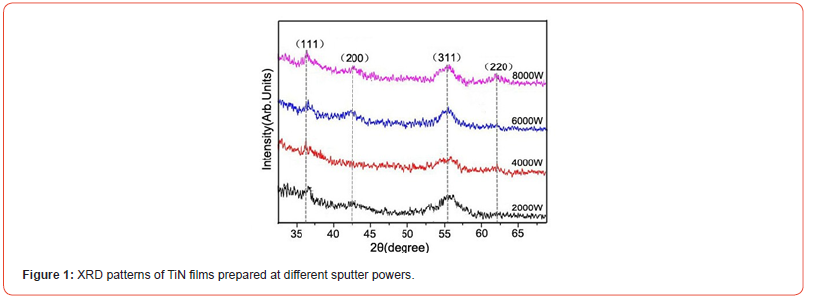
Figure 1 shows the XRD pattern of grown films prepared under different sputter powers. It can be seen from the figure that (111), (200) and (220) diffraction peaks of TiN film samples appear at 2θ=36.90, 42.90 and 62.70, respectively, indicating that the prepared TiN film has a polycrystalline face-centered structure. The highest diffraction intensity was obtained at plane (111). When the sputter power is 8 kW, the (200) and (220) diffraction peaks are strong. In addition, the (311) diffraction peak of Si substrate is also observed in Figure 1..
Figure 2(a)-(d) shows the surface topography of TiN films prepared with different sputter powers. It can be seen from the figure that the surface topography of TiN films changes greatly. When the sputter power was 2 kW, the surface of TiN film contained many small particles. With the increase of sputter power, the surface grain size of TiN film increased, and the surface grain was rough and dense, with tetrahedral structure. When the sputter power reached 8 kW, columnar structure grains appeared on the surface, and the grain size increased. Actually, the increase of sputter power leads a higher growth rate. It means a large number of sputtered particles accumulated on substrate surface, causes the formation of big grains. When the sputter power is too high, the sputtered particles carry larger energy, resulting in that the film growth and the particle combination take place together, which forms a situation of the common growth of grains of different specifications [1]. The inset in Figure 2(a) is the cross-section topography of TiN thin film at 2 kW sputtering power. It can be seen from the figure that TiN thin film has a columnar structure without obvious defect pores. The film thickness is 50 nm.
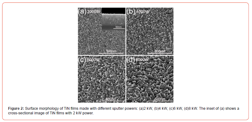
Figure 3 shows the thickness uniformity (THKU), stress, and resistivity of the grown films prepared with different sputter powers. With the increase of sputter power, the thickness uniformity of TIN films decreases from 4.30% to 3.05%, which decreases by 1.25%. The uniformity is closely related to film thickness and is an important index to measure film quality. When sputter power increases, the self-bias of sputtering increases, the energy of sputter particles is enlarged also. The bombardment effect of charged particles on the substrate enhances the migration and diffusion ability of surface atoms, resulting in higher atomic diffusion speeds on the film surface. It makes the structure of film more dense [8]. It can be seen from Figure 3 that the stress of the grown TiN film is compressive. The enhancement of sputter power on the film stress is obvious. When sputter power increases, the film stress decreases from -418.6 MPa to -652.8 Mpa. T.D. Nguyen et al found that the interfacial stress of the thin film was related to the crystal surface growth orientation and lattice mismatch in the growing process of thin film [10]. Meanwhile, in the process of DC magnetron sputtering, the film stress was related to the bombardment of high-energy particles with certain momentum. Bombardment by high-energy particles may cause relatively high interfacial stress, which may generate two driving forces of surface energy and strain energy, thus affecting the orientation and stress performance of (111) and (200) crystal planes of TiN film [11]. Therefore, the (200) peak of TiN film gradually increased (as shown in Figure 1), and the film stress decreased with the increase of sputter power.
The resistivity of TiN films varies significantly with the sputtering power, as shown in Figure 3. As the sputter power increases from 2 kW to 8 kW, the resistivity of TiN films decreases from 420.3 μΩcm to 303.5 μΩcm. Sputtering power affects the intensity of electric field between cathode target and substrate in reactive magnetron sputter process. Electric fields can directly influence the intensity of plasma and kinetic energy of particle, further affecting the content of Ti in TiN film and the deposition rate [12]. Therefore, with the increase of sputter power, the conductivity of TiN film will be improved. In addition, the resistivity of TiN film is also affected by the orientation of crystal growth. The (200) crystal surface has a low surface energy. When TiN film grows along the (200) crystal surface, the resistivity of TiN film is the lowest, because the atomic density of the (200) crystal surface is low, which would help to reducing the scattering of electrons. With the increase of sputter power, the diffraction peak strength of (200) increases, and the conductivity becomes better [4]. This result is consistent with the result reported by J. Freixas et al, they found that the resistivity of the film grown along the (200) crystal plane is lower than that along the (111) crystal plane [13].
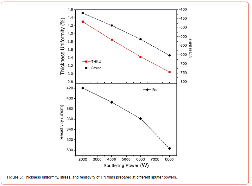
According to the above discussions, when the sputter power is 6 KW, the resistivity of TiN film sample is 360.9 μΩcm, which is still in the high resistivity range. On the other hand, the thickness uniformity (3.43%) and stress (-563.4Mpa) of the film are moderate.
Effect of Ar/N2 ratio
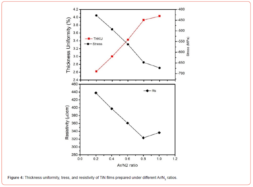
In order to evaluate the influence of the sputter gas, the flow rate of sputter gas was kept as 124 sccm and sputter pressure remained at 1.73Pa. The sputter power was set to 6 kW. Different ratios of Ar/N2 (103.3sccm, 88.6sccm, 77.5sccm, 68.9sccm and 62sccm, respectively) were applied. As can be seen from Figure 4, the thickness uniformity of TiN film samples gradually increases with the increase of Ar/N2 ratio. On the other hand, with the increase of Ar/N2 ratio, the stress (compressive stress) of TiN film sample decreases gradually. It can be seen that a moderate reduction of Ar/N2 flow ratio (increase of N2 gas flow) may result in a denser surface structure for TiN film, which is consistent with the research results of He Chunlin et al. [14]. When the working pressure remained constant and the Ar/N2 flow ratio increased, N2 partial pressure in the sputtering cavity decreased while Ar partial pressure increased, leading to an enhancement of Ti sputter rate, the TiN film grew faster. Whereas the Ti particles adsorbed on the film surface did not have enough time for surface migration. Therefore, the density and roughness of TiN film become worse [15]. With the decrease of Ar/N2 flow ratio (the increase of N2 gas partial pressure), the accumulation of TiN grains becomes more compact and neater, which makes a denser surface of the TiN film. It turned out affecting the stress in Tin film [16].
The dependence of resistivity (Rs) of TiN films on the Ar/N2 flow ratios is also shown in Figure 4. As the Ar/N2 ratio increases from 0.2 to 0.8, the resistivity of TiN samples drops from 437.8 μΩcm to 323.2 μΩcm. However, the resistivity turns out to increase to 336.6 μΩcm when the Ar/N2 ratio increases from 0.8 by 1.0. Due to the increased the content of Ar gas in the sputter cavity, the bombardment of Ar+ ions on the high purity Ti target gets stronger.
Many more Ti particles with high energy react with nitrogen atoms on the substrate. Meanwhile, the diffusion ability of high-energy Ti particles on the surface of the film becomes stronger, which leads to more oriented grains and ordered crystallization. It further reduces the defect density in grown films and improves the carrier concentration and mobility. Thus, it results in an enhanced conductivity [17]. Since the sputter power remains unchanged at 6 kW, the number of Ti atoms sputtered by Ar+ bombardment remains also unchanged. When the ratio of Ar/N2 exceeds a certain value (0.8), there are extra number of Ar+ ions may collide with the grown film as well as substrate. As a result, the structure of TiN film changes to a certain extent and the resistivity of TiN film increases [1,17]. Therefore, there might be a critical value of Ar/N2 ratio to form a more conductive TiN film. Young-Ki Lee et al. [18] believed that the adjustment of Ar/N2 ratio could affect the crystallization and distribution state of TiN in the film. With the decrease of Ar/N2 ratio, the N vacancy in TiN reduced and scattering of the electron decreases correspondingly, which may benefit to improve the mobility of electrons and change the resistivity of TiN film. The Ar/N2 ratio also affects the stoichiometric number of N content in TiNx films. A higher ration of N2 may cause target poisoning [7].
G. Lu et al. [19] found that with the increase of nitrogen content, more N atoms proportionally occupy the interstitial positions of TiN lattice, hence increases lattice constant, and decreases the thermal diffusion coefficient. It may reache a stable range. Under such conditions, TiN film may be formed with a good quality. Our results also imply that a low Ar/N2 ratio (i.e. a higher N2 content) can help to improve the growth quality, for the sputtered Ti atoms can combine with more nitrogen atoms, and fully react with them.
Influence of sputter pressures
Sputter pressure has great impact on the mean free path and energy of the gas particles. In this study, we kept the sputter power as 6 kW, the Ar/N2 ratio ~0.2, and the gas flow rate ~124 sccm. The sputter pressure was regulated by changing the pumping speed of the molecular pump. Different sputter pressures (1.47Pa, 1.6Pa, 1.73Pa, 1.87Pa and 2.0Pa, respectively) were applied to study their impact on THKU and stress formed in TiN films. It can be seen from Fig. 5 that when we reduced sputter pressure the thickness uniformity of TiN films was improved (from 3.79% to 1.55%), and the film stress (compressive stress) changed from -374 Mpa to -490 Mpa. The sputter pressure can affect the concentration of plasma in the sputtering cavity, thus controlling the kinetic energy of particles [20]. With the increase of sputter pressure, the number of particles in the sputter cavity increases, and the mean free path between par ticles decreases significantly. Ti atoms sputtered out of target could reach the substrate surface only after repeated scattering, resulting in loss of the energy of gas particles. Many particles even could not reach the substrate. The corresponding number of particles participating in the reaction dropped, and the atomic energy of sputtering to the substrate decreases. Its lateral migration and diffusion ability got poor. Many more defects such as grain boundaries were formed, lead to a rougher surface of the film [18]. Decrease of working pressure could also affect the densification and stress of the film.
It can be seen from the figure 5 that the resistivity of TiN film sample gradually increases from 397.3 μΩcm to 512.6μΩcm with the increase of sputtering pressure. According to the motion theory of gas molecules [8], when the molecular diameter and deposition temperature of sputtering gas do not change, with the increase of pressure in the sputtering cavity, the mean free path of particles decreases, and emission of secondary electrons is enhanced. Multiple collisions of Ti particles with gas molecules take place. Meanwhile, the increase of the probability of Ti particles colliding with gas molecules may enhance the scattering degree of Ti particles. It also reduces the probability of Ti particles reaching the substrate and increases the interfacial scattering of TiN film particles within a unit volume [17]. It further increases the scattering of electrons during the motion and the resistivity of grown films [18]. The resistivity of grown films also depends film thickness, preferred orientation, defect density, surface roughness and residual stress [19]. The thickness of TiN films prepared in this work is basically the same, and its resistivity increases with the increase of sputter pressure. On the other hand, the defect density and densification of film tissues may rise, which are not favourable to the electrical conductivity [21].
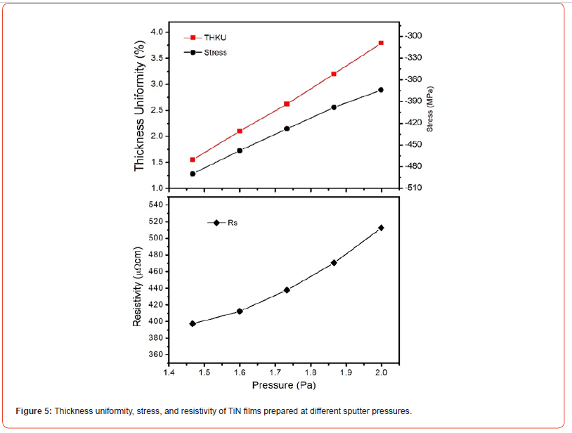
According to the above discussions, the quality of the grown TiN films can be reasonable if we use the optimized sputter conditions (sputter power ~6 kW, the ratio of Ar/N2 ~0.2, the total flow rate of sputter gas ~124sccm, and sputter pressure ~1.6Pa). The thickness uniformity, stress and resistivity of TiN film are 2.1%, -457.9Mpa and 412.4μΩcm, respectively.
Conclusion
In this paper, TiN films were prepared on monocrystal silicon substrate by DC reactive magnetron sputtering. The effects of sputter parameters (like sputter power, argon/nitrogen flow ratio, and sputter pressure, etc.) on the structure, thickness uniformity, film stress and resistivity of TiN films were studied. TiN films with good quality can be obtained with the optimal process parameters.
Acknowledgement
This work has been supported by the National Natural Science Foundation of China (11747027, 11974304, 61701434), Doctoral Program of Zaozhuang University (1020718), and contract research project (63501210615).
Conflicts of Interest
No conflict of interest.
References
- ZHANG Y, LV JF, YANG JB (2018) Effect of TiN thin film process on organic light emitting diodes. Optoelectronic Technology 38(3): 190-194.
- WANG CY, CHOU CY, SHIUE HF, Hsing-Yang Chen, Chen-Hsiang Ling (2022) Atomic layer annealing for modulation of the work function of TiN metal gate for n-type MOS devices. Applied Surface Science 585: 152748.
- TAOURIRIT TE, MEFTAH A, SENGOUGA N, Marwa Adaika, Slimane Chala (2019) Effects of high-k gate dielectrics on the electrical performance and reliability of an amorphous indium-tin-zinc-oxide thin film transistor (a-ITZO TFT): an analytical survey. Nanoscale 11: 23459-23474.
- GAO J, AARNINK WAM, GERRITSMA GJ, VELDHUIS D, ROGALLA H (1991) Preparation and properties of all high Tc SNS-type edge dc SQUIDs. IEEE Trans Magn MAG 27(2): 3062-3066.
- GAO J, KLOPMAN BBG, REITEMA AE, AARNINBK WAM, GERRITSMA GJ, et al. (1992) Epitaxial YBa2Cu3Ox thin films on sapphire with a PrBa2Cu3Ox buffer layer, Journal of Applied Physics 71(5): 2333-2336.
- GAO ZY, YANG D, SUN CJ, et al. (2023) Research progress of TiN Films prepared by magnetron sputtering technology. Hot Working Technology 52(8): 6-11.
- OLIVEIRA JC, FERNANDES F, SERRA R, A Cavaleiro (2018) On the role of the energetic species in TiN thin film growth by reactive deep oscillation magnetron sputtering in Ar/N2. Thin Solid Films 645: 253-264.
- SHI SY, MA B, XUE MY, et al. (2022) Preparation of TiN electrode films of uniform thickness with ultra-high conductivity by reactive magnetron sputtering. Materials Science and Technology 30(3): 1-6.
- LI XR, CAO Z, YU GQ, et al. (2021) Effects of N2/Ar flow ratio and substrate temperature on properties of RF-sputtered TiN film. ELECTROPLATING & FINISHING 40(23): 1776-1780.
- GAO J, WONG WH, XHIE J (1995) Formation of outgrowths at the initial growing stage of YBaCuO ultrathin films on ZrO2, Applied Physics Letters 67: 2232-2234.
- TANG WH, GAO J (1998) Influence of Nd at Ba-sites on superconductivity of YBa2-xNdxCu3Oy, Physica C 298(1-2): 66-72.
- HOU Q, GAO J (1999) Enhanced adhesion of diamond-like films with a composition-graded intermediate layer, Applied Physics A 68: 343-347.
- FREIXAS J, EUSTACHE E, ROUSSEL P, et al. (2015) Sputtered titanium nitride: a bifunctional material for Li-Ion Microbatteries. Journal of The Electrochemical Society 162(4): A493-A500.
- HE CL, GAO JJ, WANG LF, et al. (2018) Effect of N2 flow rate on microstructure and adhesion strength of reactive magnetron co-sputtered TiN/Ni nanocomposite films. Materials Reports B: Research paper 32(6): 2038-2042.
- KUMAR M, MISHRA S, MITRA R (2013) Effect of Ar:N2 ratio on structure and properties of Ni–TiN nanocomposite thin films processed by reactive RF/DC magnetron sputtering. Surface and Coatings Technology 228: 100-114.
- HU LB, GAO J, SHEN S (2003) Influence of spin transfer and contact resistances on the measurement of spin hall effect, Physical Review B 68(11): 115302.
- HU F, GAO J, WU X (2005) Controllable colossal electro resistance in La8Ca0.2MnO3 epitaxial thin films, Physical Review B 72(6): 064428.
- HU F, GAO J (2005) Current-induced asymmetric transport in La8Ca0.2MnO3 epitaxial thin films, Applied Physics Letters 87: 152504.
- BOGUSLAVSKIJ YM, GAO J, TERPSTRA D, GERRITSMA GJ, ROGALLA H (1992) Transport processes in YBCO/PBCO/YBCO ramp Josephson junctions, Physica C 194: 268-276.
- LUO Z, GAO J, DJURISIC AB, YIP CT, ZHANG GB (2008) Photoelectric response of Schottky barrier in La7Ca0.3MnO3/Nb:SrTiO3 heterojunctions, Applied Physics Letters 92: 182501.
- YEH TS, WU JM, HU LJ (2008) The properties of TiN thin films deposited by pulsed direct current magnetron sputtering. Thin Solid Films 516(21): 7294-7298.
-
WANG Junbao, XIAO Weiwei, WANG Lu, LIANG Lanju and GAO Ju*. Studies on Thickness Uniformity, Stress Modulation, as well as Transport Behavior in Sputtered thin Films of TiN. Glob J Eng Sci. 11(2): 2023. GJES.MS.ID.000756.
-
Magnetron sputtering, TiN film, Thickness uniformity, Stress, Resistivity
-

This work is licensed under a Creative Commons Attribution-NonCommercial 4.0 International License.


